Bits4Bots
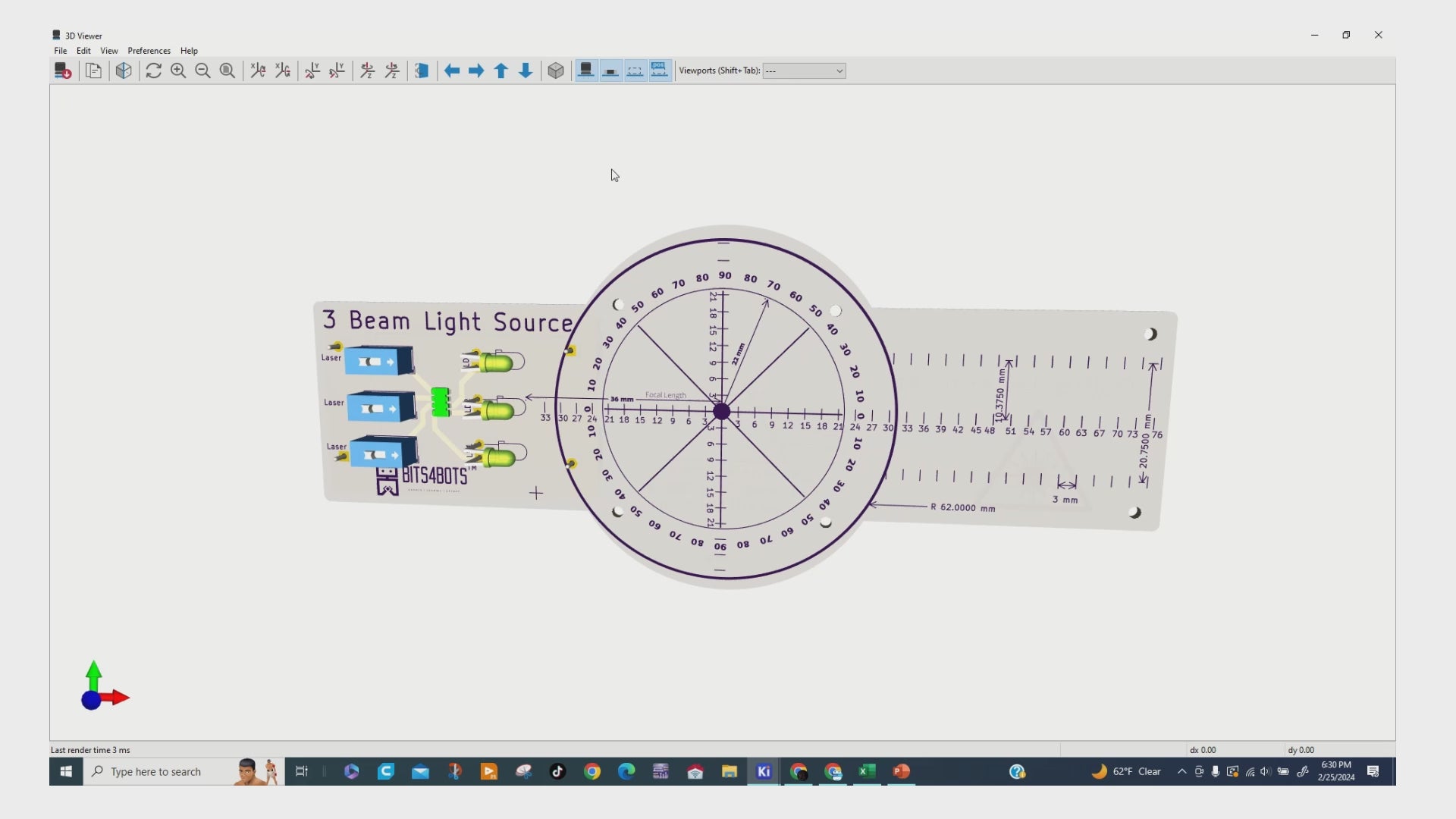
Custom 2-Layer PCB Design Service with KiCad Software
No se pudo cargar la disponibilidad de retiro
Electronics project with our custom 2-layer PCB design service. We use KiCad software.
Whether you're a hobbyist, entrepreneur, or professional engineer, our team of experienced designers is here to bring your ideas to life. From simple circuits to complex projects, we specialize in creating tailored PCB layouts that meet your specific requirements.
Key Features:
-
Customized Designs: We understand that every project is unique. Our designers work closely with you to understand your needs and create PCB layouts that precisely match your specifications.
-
KiCad Expertise: KiCad is an open-source EDA (Electronic Design Automation) software known for its versatility and robust features. Our designers are proficient in using KiCad to design high-quality PCBs that meet industry standards.
-
2-Layer Boards: Whether you need a simple 2-layer board for a prototype or a more intricate design for production, we've got you covered. Our expertise extends to all aspects of 2-layer PCB design.
-
Reverse Engineering: Have an existing circuit board that needs modifications or improvements? We welcome reverse engineering projects and can provide schematics to accompany your custom PCB design.
-
Quality Assurance: We prioritize quality at every step of the design process. Our thorough review and testing procedures ensure that your PCB meets performance standards and reliability expectations.
-
Fast Turnaround: Time is of the essence in electronics projects. With our efficient design process and dedication to meeting deadlines, you can expect a fast turnaround time for your custom PCB designs.
How It Works:
-
Submit Your Requirements: Provide us with your project requirements, including any schematics, specifications, and design preferences.
-
Consultation: Our team will review your requirements and schedule a consultation to discuss your project in detail. We'll clarify any questions and provide insights into the design process.
-
Design Phase: Once we have a clear understanding of your needs, our designers will begin crafting your custom PCB layout using KiCad software. We'll keep you updated on the progress and welcome any feedback along the way.
-
Review and Revision: Before finalizing the design, we'll conduct a thorough review to ensure accuracy and functionality. If revisions are needed, we'll incorporate your feedback to refine the design accordingly.
-
Delivery: Upon completion, we'll deliver the finalized PCB design files along with any accompanying documentation, including schematics if reverse engineering was involved.
Transform your electronic projects with our custom 2-layer PCB design service powered by KiCad. Let's bring your ideas to reality!
-
Basic PCB Design Package:
- Price: $100 - $300
- Includes:
- Up to 10 components
- Single-sided or double-sided PCB layout
- Standard PCB size (e.g., 100mm x 100mm)
- Gerber files for manufacturing
- Estimated delivery time: 1 - 2 weeks
-
Standard PCB Design Package:
- Price: $300 - $800
- Includes:
- Up to 50 components
- Double-sided PCB layout with moderate complexity
- Custom PCB size (within reasonable limits)
- Basic signal integrity checks
- Gerber files and BOM (Bill of Materials) for manufacturing
- Estimated delivery time: 2 - 3 weeks
-
Advanced PCB Design Package:
- Price: $800 - $1500
- Includes:
- Up to 100 components
- Multilayer PCB design (4 layers or more) with high complexity
- High-speed signal routing considerations
- Differential pairs routing
- Impedance control
- Thermal management considerations
- DFM (Design for Manufacturing) checks
- Gerber files, BOM, and assembly drawings
- Estimated delivery time: 3 - 4 weeks
Additional Services (Optional, priced separately):
- Schematic capture: $50 - $200 per schematic page
- Component sourcing and procurement assistance: $50 - $200
- PCB prototype fabrication and assembly coordination: Cost varies depending on quantity and complexity
Note: Prices mentioned above are indicative and may vary based on individual freelancers' rates, project requirements, and negotiation. It's essential to discuss specific project details with the freelancer to get an accurate quote.
Materiales
Materiales
Envío y devoluciones
Envío y devoluciones
Dimensiones
Dimensiones
Instrucciones de cuidado
Instrucciones de cuidado


